PCB Design & Simulation Made Easy
The Proteus Design Suite combines ease of use with a powerful feature set to enable the rapid design, test and layout of professional printed circuit boards.

Proteus
PCB Design
Proteus PCB tools seamlessly combines schematic capture and PCB layout to provide a powerful, integrated and easy to use suite of tools for professional PCB Design.
PCB Design SoftwareProteus
Circuit Simulation
Design, Test and Debug complete embedded systems inside schematic capture before ordering a physical prototype. VSM brings AGILE development to the embedded workflow.
Circuit Simulation SoftwareProteus
IoT Builder
A complete workflow for designing an Arduino™ or Raspberry Pi® appliances and then controlling it remotely from a phone or browser. Build multi-appliance systems with the MQTT protocol. Design, simulate and deploy directly from Proteus.
IoT Builder Software
Push and Shove Route Editing.
The 8.17 release is a significant point release introducing a new Push and Shove route editing mode. Building on the Push routing algorithms, users can now push tracks and vias out of the way during a route editing operation. This is fully design rule aware and works with both linear and curved cornering modes.
- Push other tracks and vias out of the way during route editing.
- Route Command Centre allows toggling of push editing mode on and off.
- Visual DRC shows clearances of objects around the mouse.
- Status bar upgrades for live display of route length and style.


Trusted in Industry and Education
35 years and counting...
We started developing Proteus way back in the days of MS-DOS. Over 35 years of constant development later we're proud to offer one of the most productive and cost effective PCB tools on the market. Our philosophy has always been one of continuous improvement and innovation resulting in a modern software suite packed full of powerful, time-saving features to help you design PCBs faster.
Affordable PCB Packages
Service and Support
Purchasing Proteus is the start - not the end - of a successful business relationship. Included with the cost of the software comes a world class technical support service. After each professional purchase one of our team will introduce themselves as your technical support point of contact. This gives you an easy way to ask questions and direct access to Labcenter support. We may not be able to solve every problem immediately but we'll certainly try our best.
Free Dedicated Support
Customer Driven Development
Our customers are the reason for our success. We remain fully engaged with our user base and encourage customers to get in touch and tell us what features would help make their job easier. We can't implement each request immediately of course but a formal logging system is in place for customer feedback which is regularly reviewed by management. Each and every Proteus product release benefits from customer driven development.
Proteus Release Features

Proteus in Education
Proteus Design Suite is found in High Schools, Colleges and Universities across the world, teaching electronics, embedded design and PCB layout to tens of thousands of students each year.
- Circuit simulation gives students a fast and fun practical learning tool.
- A software solution allows instructors to prepare and re-use virtual labs.
- Flexible licensing gives freedom for classes and assignments to be completed anywhere.

Proteus in Industry
The Proteus Design Suite is widely used across various industry sectors as a cost effective solution for professional PCB design and as a rapid prototyping tool for R&D.
- Virtual Prototyping enables system Testing before the first physical PCB is ordered.
- Shape based autorouting as standard saves time with non-critical routing.
- Direct access to over 15 million parts means never building a component or footprint again.
Proteus Resources
Learn more about the Proteus product range via the resource links opposite. You'll find lots of good tutorial movies in the video library and you can access technical brochures and the demo version from the downloads page.
More Reasons To Try Proteus
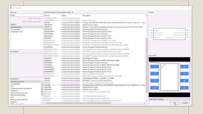
Library Parts
15 million library parts integrated and on demand.
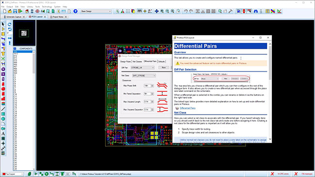
High Speed Design
Differential Pair routing and group Length Matching.

Manual Routing
Multiple routing modes provide full control when routing PCB layout


IoT
Remote front panel design for Arduino and Raspberry Pi Appliances.
Get Started for Free!
Try the Proteus Design Suite today. Our demo version is time limited only in simulation and is a great way to get started with the Proteus tools. Alternatively, if you want a full evaluation please contact the sales team via the link below.
 Ask An Expert
Have a Question? Ask one of Labcenters' expert technical team directly.